
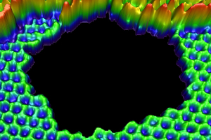
 Electron microscope image of a hole embedded within a sheet of graphene. The corners of the green hexagons are carbon atoms which form graphene’s crystal structure. Image courtesy of the Zettl Research Group, Lawrence Berkeley National Laboratory and University of California at Berkeley.
Acquiring a sample of graphene is almost comically easy. Start with an ordinary piece of graphite, which is basically the same material that is used in pencil lead. Squeeze it between two pieces of Scotch tape and tear them apart. Repeat several times until pieces of the graphite have been cleaved into sheets no more than a single atom thick. Voila - graphene! Total cost of 1 pencil plus a roll of Scotch tape: about $3.
Simple as this process is, scientists did not even know that single sheets of graphene could exist until 2004. Now that we know that we can make graphene, it turns out that it has some amazing electrical properties and someday might even replace silicon as the most important component in computer circuitry. To that end, researchers in Alex Zettl’s group at Berkeley have endeavored recently to isolate suspended membranes of graphene for study and image them at Lawrence Berkeley Lab’s TEAM 0.5, the world’s most powerful transmission electron microscope (TEM). Results were published last spring by Çaglar Ö. Girit and others in the Science.
Two aspects of the Zettl group’s recent work have been particularly interesting. First, the TEAM 0.5 microscope not only has the ability to see individual atoms of graphene, but can also take pictures in close to real time. This means that Girit was able to see dynamics of graphene as they actually happened. Other types of microscopy (scanning tunneling microscopes, for example) can take several minutes to get a single picture.
Second, Girit and others centered their images at a hole within the graphene sheet. This allowed them to observe the dynamics that occur at the material’s edge. Such edges can have a notable effect on a graphene sheet’s electrical properties and thus understanding them and controlling them would be crucial in the design of any future technology.